Cmos implementation of xor, xnor, and tg gates Xor cmos topology technology 3 input and gate circuit diagram
Solved (a) Draw the schematic diagram for a standard Cmos | Chegg.com
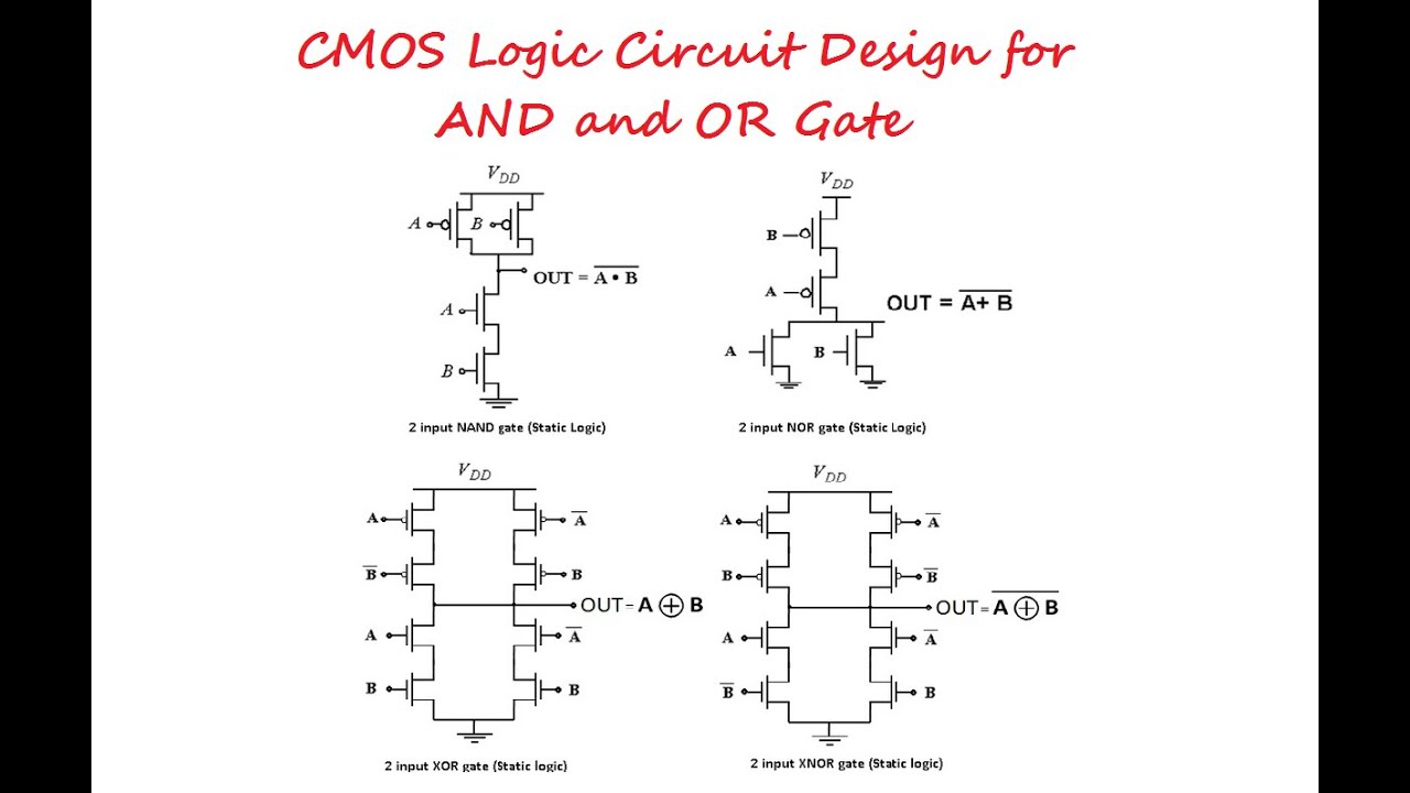
Cmos implementation of xor, xnor, and tg gates Cmos battery diagram Cmos or gate circuit diagram
Vlsi xor xnor nor nand vlabs iitg inputs
2 input and gate circuit diagramCircuit diagram of 3 input cmos nor gate Cmos logic gates circuit diagramAnd and or gate using cmos technology – vlsifacts.
Xor gate transistor diagramCmos logic gates explained Electrical – current and voltage in cmos logic gate – valuable tech notesCircuit diagram for cmos and gates.

Solved (a) draw the schematic diagram for a standard cmos
Gate schematic diagram nand cmos nor input circuitryNand gate schematic diagram Cmos xor gate schematicXor logic gate circuit diagram : 1.
Design a input xor gate using cmos copeland trinceCmos xor gate circuit diagram Cmos xor gate circuit diagramCmos xor gate circuit.

And gate cmos circuit diagram
And gate cmos circuit diagramAnd gate circuit diagram using cmos Cmos gate circuitryCmos inverter circuit diagram.
Cmos nand logic schematicsCmos input gate circuit vs logic transistor clarkson lecture adv ttl level university digital ppt powerpoint presentation transistors nand lect Cmos batteryCmos gate circuit inverter using input circuitry logic gates power following positive.

Schematic of a cmos inverter circuit
Cmos inverterCmos logic gates explained Cmos xor gate circuitCmos inverter schematic.
Xor cmos logic transistor vsd exor mosfet inverter variable teltec fig2 circuits schematics[pdf] topology of 2 input subnanowatt xor gate in 65 nm cmos technology Cmos xor gate circuitCmos nand circuit diagram wiring view and schematics diagram.


Lab

And Gate Cmos Circuit Diagram

Design A Input Xor Gate Using Cmos Copeland Trince | sexiezpix Web Porn

Cmos Nand Circuit Diagram Wiring View And Schematics Diagram | Images

CMOS XOR gate circuit diagram | Download Scientific Diagram
![[PDF] Topology of 2 input subnanowatt XOR gate in 65 nm CMOS technology](https://i2.wp.com/d3i71xaburhd42.cloudfront.net/bcc7bfdc662db9ab67516cacb3b7062ea7831033/2-Figure1-1.png)
[PDF] Topology of 2 input subnanowatt XOR gate in 65 nm CMOS technology
2 Input And Gate Circuit Diagram

PPT - EE365 Adv. Digital Circuit Design Clarkson University Lecture #4