Cmos logic gates explained Nand gate cmos diptrace pcb layout Cmos nand gate nor
Nand Gate Diagram
Cmos nand circuit diagram Cmos logic circuit design for not, nand and nor gate Nand layout gate simple laying circuits larger version figure click
Layout nand lab gate nor input xor using schematic gates
2 input nand gate cmos schematicNand cmos gate Nand and nor gate using cmos technology – vlsifactsNand gate schematic diagram.
Circuit diagram of cmos nand gateSettlers motto auction 3 input nand gate truth table see through Cmos nand gate circuit diagram[diagram] circuit diagram nand gate.

Cmos nand gate
Nand gate cmos diptrace pcb layoutCmos nand Stick diagram of two input cmos nand gate || compact stick diagramCircuits intégrés logiques c-mos.
A cmos nand gate. b cmos nor gate. c equivalent impedance circuitsCmos nand gate Cmos nand circuit diagramCmos nand circuit diagram.

[diagram] circuit diagram nand gate
3 input and gate circuit diagram2 input nand gate cmos schematics pdf Nand logic cmos ttlCircuit diagram of nand gate.
Nand gateCmos nand gate circuit diagram Nand gate layoutCmos nand circuit simulator.
![[DIAGRAM] Circuit Diagram Nand Gate - MYDIAGRAM.ONLINE](https://i2.wp.com/circuitdigest.com/sites/default/files/circuitdiagram/NAND-Gate-Circuit-Diagram.gif)
Nand gate internal circuit
Nand gate diagramCmos nand gate circuit diagram E77 . lab 3 : laying out simple circuits.
.

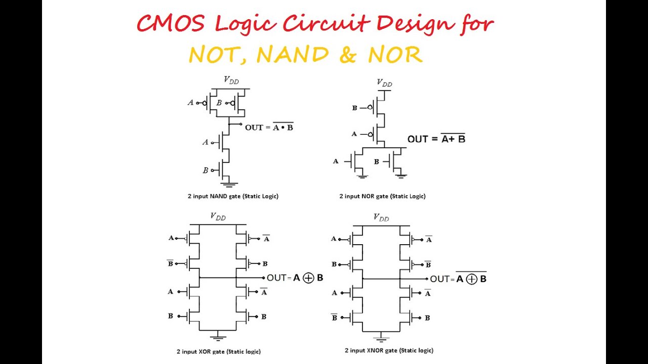
CMOS Logic Circuit Design for NOT, NAND and NOR Gate - YouTube

Nand Gate Diagram

NAND Gate

Nand Gate Cmos Diptrace Pcb Layout

3 Input And Gate Circuit Diagram

Lab6 - Designing NAND, NOR, and XOR gates for use to design full-adders

stick diagram of two input CMOS nand gate || compact stick diagram
![[DIAGRAM] Circuit Diagram Nand Gate - MYDIAGRAM.ONLINE](https://i2.wp.com/www.researchgate.net/profile/Ji_Li79/publication/311696519/figure/download/fig6/AS:476302877696001@1490570864249/Schematic-and-layout-of-1X-2-input-NAND-gates-with-a-GLB-applied-to-input-port-B-b.png)
[DIAGRAM] Circuit Diagram Nand Gate - MYDIAGRAM.ONLINE